August 23, 2025, by Helen, Special Editor for C-FOL
Introduction
Wafer-level testing of Photonics Integrated Circuits (PICs) is a complex interdisciplinary systems engineering discipline, integrating precision machinery, optical design, automatic control, and software algorithms. Sunyu Photonics’ solution directly addresses the core pain points of PIC wafer testing. Through integrated innovation of optoelectronics, software, and machinery, it has successfully resolved industrialization challenges of edge-coupling technology in terms of precision, efficiency, and reliability. This provides critical testing support for large-scale PIC mass production and is expected to accelerate the development of the entire photonics integration industry.
Co-Packaged Optics (CPO), a key technology to break through AI computing power bottlenecks, significantly improves transmission speed and energy efficiency by co-packaging optical engines with chips. It has become a core development direction for supercomputing and AI computing centers. As the functional carrier in CPO and traditional optical chip packaging, PIC performance directly impacts system performance. Wafer-level testing is particularly crucial for CPO: by verifying PIC stability, consistency, and reliability, it lays the foundation for efficient integration and yield improvement. Currently, facing challenges such as multi-physical field integration and high-density packaging, wafer testing still lacks systematic, efficient, and high-precision solutions. This has become an industrial bottleneck restricting large-scale application of CPO and high-end PIC technologies, urgently requiring breakthroughs.
1. Challenges in PIC Wafer Testing
PIC wafer testing is a core process to ensure the performance and reliability of PIC devices. Its goal is to identify and eliminate underperforming chips before packaging, avoiding high packaging and testing costs for defective products, while providing direct, fundamental data support for wafer process optimization and yield improvement. Compared with traditional electrical chip testing and single-PIC testing, PIC wafer testing faces unique challenges in the following aspects:
1.1 Ultra-High Requirements for Optical Alignment Precision
The coupling efficiency of optical signals highly depends on sub-micron precision alignment between fiber probes and waveguide endfaces across six degrees of freedom (X, Y, Z translations and Rx, Ry, Rz rotations), while ensuring high repeatability of optical signal coupling. Traditional electrical probes only require vertical contact, but optical testing demands approach at non-orthogonal angles. The alignment process is complex and prone to collisions, placing extremely high demands on mechanical systems and control algorithms.
1.2 Measurement Interference from Process Variations
When scaling from single-chip R&D to full-wafer testing, process variations—such as uneven silicon thickness, etching line width fluctuations, overlay errors, and wafer warpage—become non-negligible factors. These variations shift the optimal coupling position of each chip. If the test system cannot automatically identify and compensate for these deviations, it will be difficult to distinguish between the device’s actual performance and coupling errors, leading to misjudgment of yield.
1.3 Complexity of Multi-Domain System Integration and Coordination
Optical testing requires integration of multiple subsystems, including high-precision motion platforms, optical probes, electrical instruments, machine vision, and temperature control modules. These systems must achieve hardware triggering and data synchronization at the microsecond level. The lack of a unified software architecture and communication standards further increases the complexity and cost of system integration and post-maintenance.
1.4 Test Throughput as a Mass Production Bottleneck
Optical coupling is a serial, time-consuming process. Each test point requires optical power searching and optimization, and traditional manual or semi-automatic solutions can take several minutes per point—far unable to meet the efficiency requirements of mass production.
1.5 Strong Dependence on Calibration and Poor Repeatability
Optical test results are highly susceptible to environmental disturbances and mechanical repeatability. Repeated loading/unloading of wafers introduces pose deviations. Without a Standard Operating Procedure (SoP) for calibration, the comparability and reliability of test data cannot be guaranteed.
2. Optical Coupling Methods and Optical Probe Types in PIC Wafer Testing
2.1 Optical Coupling Methods
Optical signals in PICs are typically transmitted horizontally. In optical engines such as CPO, coupling between PICs and other active/passive devices is also horizontal. To evaluate the function and performance of optical paths in PICs, optical coupling in PIC wafer testing mainly includes two methods—surface coupling and edge coupling—depending on the material platform and chip structure.
- Surface Coupling (Vertical Coupling Based on Diffraction Gratings)
This method uses diffraction gratings to redirect horizontally transmitted test optical signals in the wafer by 90°, enabling vertical coupling with the wafer surface. Leveraging the diffraction effect of gratings, periodic gratings are fabricated on the surface waveguides of the chip. At the input port, incident optical signals strike the wafer surface vertically; when the phase matching condition is met, light can be efficiently coupled into horizontal waveguides. At the output port, outgoing signals from horizontal waveguides are diffracted by gratings to exit vertically from the wafer surface.
This method is mature and widely used in silicon photonics and silicon nitride platforms, with relatively easy implementation of test systems. However, it has key drawbacks:
- Edge Coupling
Suitable for structures with exposed waveguide endfaces or embedded deep grooves (e.g., InP edge emitters or silicon photonics inverse taper structures). Incident and outgoing optical signals are directly coupled with optical probe arrays at waveguide endfaces with high precision, and measurements are performed using optical signals from the probes. Optical probes are typically manufactured via methods such as polished arrayed fibers or 3D-printed microlenses.
This method aligns with the coupling mechanism between PICs and other components, resulting in more direct and accurate test results. Edge coupling offers advantages of high bandwidth and low loss. Its key challenges lie in achieving precise probe alignment and improving coupling efficiency. Implementing edge coupling at the wafer level also requires etching deep coupling grooves at the input/output endfaces of chips on the wafer.
Due to its directness, accuracy, and low overall cost—and since pre-etching coupling grooves for chip testing on wafers is inexpensive—edge coupling has become the mainstream trend for high-bandwidth PIC testing.
2.2 Types of Optical Probes
Common optical probes mainly fall into three categories:
1. Planar Lightwave Circuit (PLC) Probes
Based on silicon or silicon nitride materials, PLC probes route optical paths to chip edges with high precision. Their mode field size can match that of PIC waveguides, enabling high port density and parallel testing—making them suitable for large-scale mass production. However, they have high manufacturing costs, require customization for specific PIC layouts, and have long design cycles and low flexibility.
2. 3D-Printed Optical Probes
Using two-photon polymerization technology, these probes integrate micro-optical structures (such as Total Internal Reflection (TIR) mirrors and aspherical lenses) on fiber endfaces, enabling efficient and precise edge coupling. However, their polymer materials have poor thermal stability, and channels are prone to drift—limiting their application in scenarios requiring long-term stability.
3. Polished Fiber Array Units (FAUs)
Through precision processing, FAUs control the curved surface topography and smoothness of fiber endfaces, achieving optimal matching with nanowaveguides and extremely low insertion loss. Constructed from all-glass/silicon materials, FAUs have an extremely small coefficient of thermal expansion, maintaining stable optical performance even under temperature fluctuations or mechanical stress.
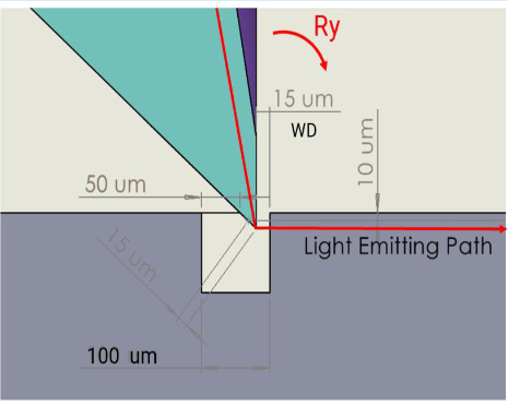
The shallow insertion depth of FAUs allows the use of smaller coupling grooves, simplifying etching processes and reducing costs while improving safety in automated operations (see Figure 1). Additionally, the design of test platforms requires optimizing FAU angles to ensure safe insertion into grooves, correct optical path direction, and precise alignment between fiber channels and optical ports on the wafer.

Figure 1: Schematic diagram of coupling between FAU optical probes and PIC grooves for PIC wafer edge testing (Dimensions: 15 μm, 50 μm, 100 μm; Optical Path: Light Emitting Path)
3. Sunyu Photonics’ Systematic Innovative Solutions
Wafer-level PIC testing requires integration of optical, electrical, and mechanical systems. The coordinated operation of these multi-domain systems is key to achieving efficient, reliable testing. To address the significant challenges of multi-domain coordination, Sunyu Photonics has launched a highly integrated, intelligent automated test system based on edge coupling. This system significantly improves test repeatability, throughput, and reliability, providing strong support for PIC R&D and mass production.
3.1 Optimized Design of Polished FAUs for Edge Coupling
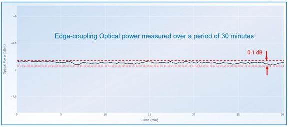
Adopting the edge-coupling technical route, Sunyu leverages its advantages of high fidelity, high bandwidth, and low loss. The company uses self-optimized polished FAUs as core optical probes. Their excellent thermomechanical stability (optical power fluctuation < 0.1 dB within 30 minutes, see Figure 2) and repeatable coupling performance lay a solid foundation for automated mass production testing.

Figure 2: Coupling stability of polished FAU optical probes in edge testing (Y-axis: Optical Power (dB); X-axis: Time (min); Fluctuation Range: 0.1 dB)
3.2 Multi-Level Fully Automated Calibration Process
Calibration is critical to ensuring the accuracy of test results. In wafer-level testing, calibration must cover optical probes, motion platforms, and test instruments. Precise calibration eliminates system errors and improves the reliability and repeatability of test results. The design and implementation of calibration processes are key to test system performance.
Sunyu Photonics has integrated a comprehensive calibration process as the cornerstone of high-repeatability testing. This process ensures that test variations remain within 0.2 dB even after wafer reloading.
Calibration typically includes top camera calibration, motion platform calibration, wafer calibration, and Z-plane calibration:
The specific calibration steps are as follows:
This fully automated calibration system effectively compensates for wafer process variations and mechanical repeatability errors, ensuring each test is performed under optimal conditions:
3.3 Intelligent Software Platform and High-Speed Algorithms
Navigo is Sunyu Photonics’ proprietary integrated software system for PIC testing, specifically designed to handle multi-physical domain parameter interaction and process control in automated PIC wafer testing. Navigo seamlessly manages complex interactions between motion platforms, optical probes, electrical instruments, and vision systems, ensuring coordinated operations across optical, electrical, mechanical, and thermal domains. This software platform serves as the "intelligent brain" of the entire automated test system.
Its integrated high-speed gradient search algorithm reduces optical alignment time to 3–4 seconds, completely resolving the efficiency bottleneck of edge coupling. Test data shows the system can complete 520 test points in 125 minutes, with an average of only 14 seconds per point (including platform movement, fiber alignment, and wavelength scanning)—significantly improving PIC mass production efficiency (Units Per Hour, UPH).
Key features of Navigo include:
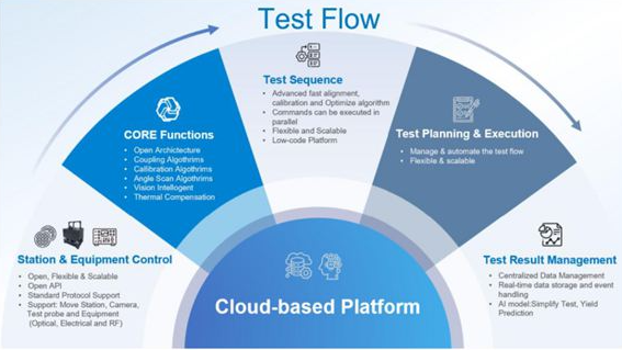
Navigo’s modular, scalable software platform is specifically designed for complex PIC wafer-level testing (see Figure 3 for the test flow).

*Figure 3: Modular and Scalable Navigo Software Architecture Based on Cloud Platform
3.4 High-Stability Hardware Platform and Automated Expansion
The PS300 Test Platform offers sub-micron positioning accuracy (< ±1.5 μm) and high mechanical stability. An optional fully automated wafer loader enables unmanned operation, eliminating human error and ensuring test consistency and efficiency in mass production environments.
Wafer-level testing of PICs is a complex interdisciplinary systems engineering discipline, integrating precision machinery, optical design, automatic control, and software algorithms. Facing core challenges such as optical alignment, process variations, system integration, test efficiency, and repeatability, Sunyu Photonics’ solution directly addresses the pain points of PIC wafer testing. Through integrated innovation of optoelectronics, software, and machinery, it has successfully resolved industrialization challenges of edge-coupling technology in precision, efficiency, and reliability. This provides critical testing support for large-scale PIC mass production and is expected to accelerate the development of the entire photonics integration industry.