The maturation of silicon optical technology towards maturity is becoming more and more evident at the recent OFC2024. This maturity is reflected in many key details, one of which is the coupling of silicon optical chips to optical fibers. Recently found a 2020 Tsinghua University Shenzhen Research Institute Xin Mu et al. wrote a review article: "silicon optical integrated chip edge coupler review", organize a few key points to learn, but also for your reference.
First look at the conclusion of the article: "Recent research work has confirmed the value of silicon optical technology in the realization of the photonic integrated chip field. In order to realize effective data transmission, optical interconnection based on silicon optical technology is a key issue. The two main chip-to-fiber coupling mechanisms, vertical coupling and edge coupling, have their own advantages and disadvantages. In contrast, edge coupling has higher coupling efficiency, wider operating bandwidth, and lower polarization correlation. This article firstly starts from the research background and application of silicon optical fiber-to-chip coupler, discusses its working mechanism, design principles, summarizes the performance of existing edge couplers, and classifies and analyzes in detail the structural variations of edge couplers in the horizontal and vertical directions. A simple comparison between edge couplers and grating couplers is also made, and encapsulation is discussed. Finally, the article also discusses issues in some experiments on edge couplers, including polarization operation, multilayer integration platforms, and inverse design methods."
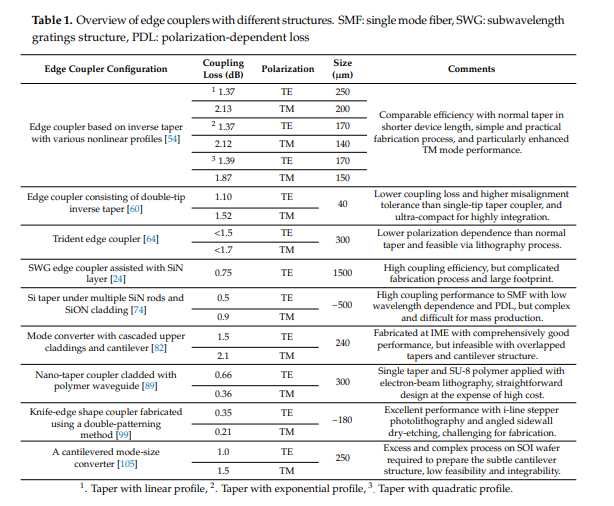
Second, let's go to the current research progress on silicon optical edge couplers mentioned in the article. As shown in the table below, the best coupling efficiency reaches more than 95% (0.21dB), but of course may face manufacturing challenges. It can also be seen that there has been more than one experimental result with less than 1dB loss. Here, the authors particularly remind the treatment of the chip end face and the design of the fiber and chip connectors (matching fluid and distance).

Third, about the comparison with vertical coupling (mainly grating coupling). The advantages of grating coupling mainly lie in the convenience of wafer testing, flexible alignment and measurement mechanisms, and smaller size. However, its disadvantages are also obvious, mainly loss (grating inherent diffraction and scattering), narrow bandwidth (grating itself with filtering effects), and is polarization sensitive. Although there are ways to overcome these problems, they inevitably introduce more complex structures. In contrast, the disadvantages of the edge coupler mainly lies in the inconvenience of wafer testing (high alignment accuracy, only in the chip end face coupling), as well as the size of the larger, part of the structure of the manufacturing process is also very complex.
Fourth, although the article is mainly about the edge coupler, but taking into account the actual packaging of optical devices, but in the recommended grating coupling. Grating coupling has a larger mode field diameter MFD, convenient and single-mode fiber coupling, also suitable for multi-fiber coupling. Why edge coupling performance is good but not popular, one reason is that edge coupling inherently low mismatch (1550nm near, 2 micron change will bring more than 1dB loss), another is the fiber end face and chip end face processing is more troublesome. Solutions include the introduction of HNA high numerical aperture fibers, and the use of V-grooves (but with larger dimensions).
To be continued, please stay tuned.

